Synthesis and Electrical, Optical, Electrochemical Properties of Chemically Deposited PbS Thin Films
A. B. Gite1*
1SNJBs KKHA Arts, SMGL comm. And SPHJ Sci College, Chandwad , Nashik India .
http://dx.doi.org/10.13005/OJPS03.01.03
Lead Sulphide (PbS) thin film was deposit by chemical bath deposition (CBD) process on the glass substrate at room temperature for various time intervals. The precursors used for this deposition are lead acetate since as a supply of lead ions (Pb2+) and thiourea the same as the supply of sulfide ions (S2-) with 0.1M concentration. The pH of the mixed precursors solution was maintained at 9.5-10 by addition of drop by drop ammonia very slowly. The cause of deposition time for different hours studied. The influence of deposition time on properties of PbS film was investigated. The color of films appears black-gray after taking out of the bath. The thickness of the film is increased with increase in deposition time. The electrical resistance and resistivity were 500MΩ and 18.75 MΩ-cm and band gap measured as a function of temperature using D.C. four probe methods was 0.3742 eV. The Cyclic Voltammetry (CV), Linear Sweep Voltammetry (LSV), Chronoamperometry were studied by using potentiostat.
Copy the following to cite this article:
Gite A. B. Synthesis and Electrical, Optical, Electrochemical Properties of Chemically Deposited Pbs Thin Films. Orient J Phys Sciences 2018;3(1).
DOI:http://dx.doi.org/10.13005/OJPS03.01.03Copy the following to cite this URL:
Gite A. B. Synthesis and Electrical, Optical, Electrochemical Properties of Chemically Deposited Pbs Thin Films. Orient J Phys Sciences 2018;3(1). Available from: https://bit.ly/3rrNzOv
Download article (pdf) Citation Manager
Introduction
CBD method is a method due to which we can deposit metal Chalcogenide thin films is receiving a great importance because of its reduction in low cost and production of high-quality material. Lead Chalcogenide is important materials with the wide variety of application including spectrometer detector, IR detector,13 etc. Among them, CBD is an economical and simple technique enables for large-scale deposition.14 In this method, growth can be easily controlled by controlling concentration of ions, bath temperature, pH, etc. Compared to other deposition methods, CBD offers different advantages such as it is the very simple method for deposition, reproducibility, harmless, cost effectiveness etc. In CBD method various preparative parameter as a temperature of deposition, concentration of precursor, bath pH, time of deposition etc15 was optimized to get uniform and well adherent PbS thin films.and pollution monitor1. PbS is a significant direct narrow bandgap semiconductor material with an estimated energy band gap of 0.37-0.4eV at 300K.2,4 PbS thin films have been widely used in a variety of fields such as a light emitting diode, solar energy panel, gas sensors, infrared detector and mid-infrared lasers.4,5 The huge excitation Bohr radius of PbS (about 0.18 nm) results in strong quantum confinement of both hole and electron in nano-size structure so that the band gap size can be control by modifying the size of the particle according to effective mass model. This property of PbS makes it desirable for new application such as solar cells.6,7 PbS thin films deposited by SILAR method and effect of pH and transport, optical properties8 can be obtained by several methods such as electrodeposition9 and PbS sensitized photoanodes were studied by the different groups,10 solvothermal,11 SILAR12 and CBD
this way, many films are immersed in 3Glass slides with the size of 75 × 25 ×2 mm are used as the substrate. In the CBD process, clean-up of the substrate surface is significant due to the surface effect on different adherent properties of the thin film. First, the substrates were cleaned with hot distilled water after it was washed with acetone. Finally, the glass slide is dried under Infrared (IR) lamp for 10 minutes. 0.1M of Lead acetate (PbAs2)[Pb(CH3(COO)2] and 0.1M of thiourea, SC (NH2)2] were used as sources of Pb+2 and S-2 ions in the solution to form nano-crystalline PbS thin films. Molar concentrations of Pb2+ and S-2 ion sources with the proportion of Pb:S (1:1) were used to form the thin film. The pH in all solutions was measured by digital pH meter and it was fixed at 10.5 using ammonia, and the total solution volume was 60mL at room temperature
Materials and Methods
Different bath containing precursors of lead and sulphide electrolyte whose pH is 10.5 for 2hrs-24hrs and each slide was placed in beaker with 45 degree angle. From observations and testing of the film growth with multimeter, we get the uniform well adherent film at 22 hr. Hence a film was deposited for 22 hr in solution. At the end of deposition time, the substrate coated with PbS on both sides are taken out from the solution and rinsed in double distilled water. Mirror-like thin film surface was obtain with gray-black color3. The electrical resistivity and band gap are by obtained by using four probe methods. The study of CV, LSV, and Chronoamperometry is done by using potentiostatic. Figure 1(a) shows the experimental set up for CBD method and Figure 1(b) shows the well adherent films obtained at different deposition time durations.
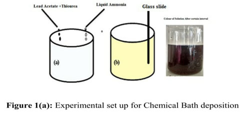 |
Figure 1a |
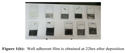 |
Figure 1b |
Characterization
The UV–Vis. absorbance spectra of the samples are recorded using a spectrophotometer (JASCO V-670). The electrical resistivity was measured by four probe apparatus and I-V characterization was done with the static gas sensing unit and all the electrochemical measurements was done with K-LYTE 1.2 Kanopy Techno solutions software designed to control the potentiostat unit with Ag/Agcl as a reference electrode (RE) and Platinum (Pt) as working electrode (WE) and Platinum (Pt) mesh as counter electrode (CE) for a bath.
Result and Discussion
The formation reaction mechanism and Electrical, optical and electrochemical characterizations of the films obtained are discussed below.
Reaction Mechanism
The result for formation of PbS thin film is also explained by various groups as [16]
Pb(CH3COO)2.3H2O → Pb2+ +3H2O+2CH3COO1-
Pb2++4NH3 → Pb(NH3)42+
SC(NH2)2+2OH- → S2-+CH2N2+2H2O
→ -+2OH2)2+SC(NH2+4)3Pb(NHPbS +4NH3+CH2N2+2H2O
The color of solution changes on addition of dropwise ammonia. This means the formation of reaction begins. The PbS films were deposited for various time durations and the deposition temperature is 300K17. At room temperature, the ions will get sufficient time to condense on the glass substrate surface so that we get a large amount of material is deposited on the substrate.
Electrical properties
I-V Characteristics of Film
In the present study, the four-point probe technique was used for the study electrical behavior ofPbS films. The resistivity measurement of PbS films deposited onto glass substrate was carried with four probe apparatus and film gives the Ohmic behavior. Variation of the voltage (mV) and current in (µA) for deposited film is as shown in Figure 2. The behavior of the film was linear in nature and it shows the resistance of 500MΩ at room temperature.
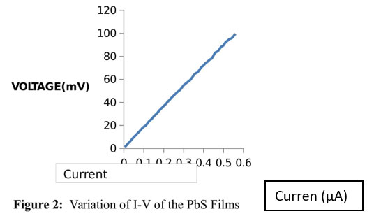 |
Figure 2 |
dc electrical resistivity
The dc electrical resistivity of the films are measured by various groups18 and hence same is used for PbS thin film was measured as a function of temperature (1000/T). Figure 3. Shows the variation of resistivity against temperature for PbS thin film was measured as a function of temperature in the range 300 to 500 K19. The variation of log ρ with reciprocal of temperature, it is observed that the resistivity is decreased with increase with temperature20, suggesting the semiconductor performance of PbS thin film. Resistivity decreases with increase in temperature which is one of the common observations in semiconducting thin films21. A room temperature electrical resistivity of metal oxides and metal Chalcogenide are determined22 for PbS thin film was obtained 18.75 Ω cm.
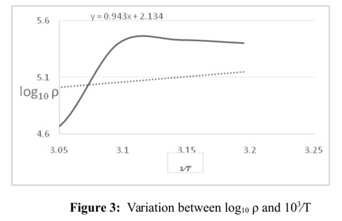 |
Figure 3 |
BadBand gap
For finding the band gap of a semiconducting material the four probe method is used. Firstly the current and voltage is measured across the lead acetate thin film at different value of temperature. From resistivity be obtained by using relation ρ = (V/I) * [ 2πs / (w/s) ] in which V is the floating potential difference between different inner probes while I is current through outer two probe and S is the spacing between two probe23. The variation of semiconductor resistivity with temperature is inferred by plotting a graph between log of resistivity, log10ρ and reciprocal of temperature 10
3⁄T .From readings a plot is obtained. From this plot a slope is obtained and by this a band gap of PbS film is calculated the formula for band gap is
Eg =2.3026*103*2*k*slope
Where, K= Boltzmann constant = 8.617*10-5eVk-1 Eg= Band gap =0.3742 eV (from calculation).
UV Visible Spectroscopy
The UV–Vis. absorbance spectra of the samples are recorded using a spectrophotometer (JASCO V-670) as shown in figure 4. and absorbance against wavelength is plotted and we get the sharp peak at the 1150nm region which gives the bulk gap of material formed as PbS.
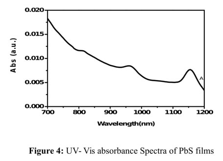 |
Figure 4 |
Electrochemical measurements
Electrochemical measurements was done with K-LYTE 1.2 Kanopy Techno solutions software designed to control the potentiostat unit with Ag/Agcl as RE and Pt as WE and Pt mesh as CE for an bath
Cyclic voltammetry
In CV the voltage is changes between two values with fix rate. When voltage reaches highest value then the scan is reversed and voltage is swept back to lowest value. CV of Pb2+ and S2- was carried out from maximum voltage 0.6V to minimum voltage -0.6V with respect to Pt as working electrode and Pt(mesh) as counter electrode. All the potential were measured against Ag/AgCl electrode, which served as reference electrode. All the experiments were carried out at room temperature. The concentration of solution which is used for CV was 0.1M.CV was taken at sweep rate of 50.00mV/s. The starting and returning potential were 0.00V and 0.00V respectively.CV shows oxidation of S2- at 0.3V and reduction of Pb2+ at 0.58V. The gap between irreversible cathodic and anodic peak increases with decreases in size indicates the quantum confinement effect .Hence it is being revealed that quantum confinement effect can be observed in the as synthesized PbS films.
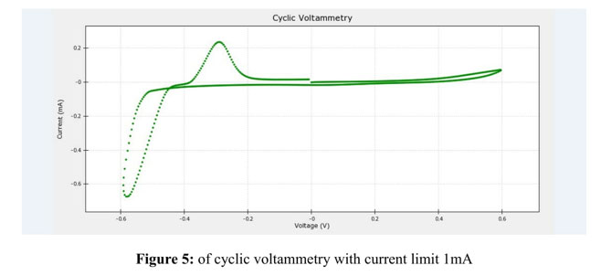 |
Figure 5 |
The reaction is,
Pb4+ + 2e- → Pb2+ E0= -0.13V
S + 2e- → S2- E0 = 0.48V
Linear sweep voltammetry (LSV)
The current at a working electrode is measured and potential between working electrode and reference electrode is swept linearly with time in LSV method and the voltage is scanned from a lower limit to an upper limit. The studies of Pb2+ and S2- was carried out from starting voltage at 0.00V and ending voltage at 1.0V with sweep rate 50.00mV/s. The scan starts from left hand side of current plot where no current flows through the solution. As the voltage is swept further to right value means more reduction of ions in the solution that is a current begins to flow and reaches a highest peak value before dropping. There is reduction of Pb4+ to Pb2+.
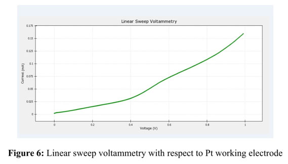 |
Figure 6 |
Chronoamperometry
In certain electrochemical technique where potential of working electrode is stepped to a constant value and results the current in a faradic process happening at substrate electrode is monitored as a time function for the process taking place at the electrode. For experiment carried out reference electrode was Ag/Agcl and working electrode was Pt. The potential of working electrode in three electrode configurations24,25 was proscribed by k-lyte 1.2 software and current was follower with rise of time. It is a single potential step in which only current resulting from forward step. In Chronoamperometry current is usually monitored vs. time. In this expt charge is monitored at working electrode. The voltage was fixed during experiment at 0.200V.
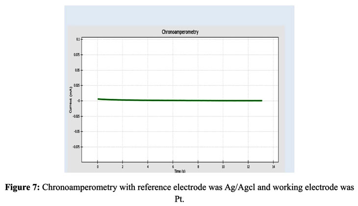 |
Figure 7 |
Conclusions
Nano-crystalline PbS film is produced by using CBD method on cleaned glass substrate at 22hrs at room temperature. During research it is observed CBD method is a cost effective method for the synthesis of the thin film. The organize way to add the reactants of precursors solutions is important. The films show the ohmic nature and the obtained band gap is 0.3742eV. The selection of precursor solution also plays a great role in formation of the films. The resistance values of PbS films can be measured using four probe method it means that the films are conductive in nature. The resistivity is found to be 18.75Ω.cm .The band gap is obtained at room temperature about 0.37eV.The good quality results are obtained of CV, LSV, and Chronoamperometry by using k-lyte potentiostatic.
Acknowledgments
This work was financially supported by physics department, SNJB ACS College, chandwad. I am grateful thanks of Principal Dr. G. H. Jain for his friendly guidance and encouragement and providing the necessary facility to carry out this research work.
References
- N. Choudhury, B.K. Sarma, Structural characterization of nanocrystalline PbS thin films synthesized by CBD method, Indian J. Pure Appl. Phys. 46) 261–265.
- S. Seghaier, N. Kamoun, R. Brini, A.B. Amara, Structural and optical properties of PbS thin films deposited by chemical bath deposition, Mater. Chem. Phys. 97 (2006) 71–80. doi:10.1016/j.matchemphys.2005.07.061.
- A.S. Obaid, M.A. Mahdi, A. Ramizy, Z. Hassan, Structural properties of nanocrystalline PbS thin films prepared by chemical bath deposition method, 2012. doi:10.4028/www.scientific.net/AMR.364.60.
- N.O. Balayeva, O.O. Askerova, A.A. Azizov, R.M. Alosmanov, G.M. Eyvazova, M.B. Muradov, Synthesis of CuS and PbS nanocrystals on the basis of PE/NBR polymer/elastomeric composites for their applications, Compos. Part B Eng. 2013; 53 391–394. doi:10.1016/j.compositesb.2013.05.049.
- S. Das, Optimisation of porosity of 7075 Al alloy 10 % SiC composite produced by stir casting process through Taguchi method Rajesh Kumar Bhushan and Sudhir Kumar *, Mater. Eng. 1 (2009) 116–129. doi:10.1504/IJMATEI.2009.024031.
- A.S. Obaid, M.A. Mahdi, Y. Yusof, M. Bououdina, Z. Hassan, Structural and optical properties of nanocrystalline lead sulfide thin films prepared by microwave-assisted chemical bath deposition, Mater. Sci. Semicond. Process. 16 (2013) 971–979. doi:10.1016/j.mssp.2013.02.005.
- D. Kumar, G. Agarwal, B. Tripathi, D. Vyas, V. Kulshrestha, Characterization of PbS nanoparticles synthesized by chemical bath deposition, J. Alloys Compd. 484 (2009) 463–466. doi:10.1016/j.jallcom.2009.04.127.
- K.C. Preetha, K. V. Murali, A.J. Ragina, K. Deepa, T.L. Remadevi, Effect of cationic precursor pH on optical and transport properties of SILAR deposited nano crystalline PbS thin films, Curr. Appl. Phys. 12 (2012) 53–59. doi:10.1016/j.cap.2011.04.040.
- R.S. Patil, H.M. Pathan, T.P. Gujar, C.D. Lokhande, Characterization of chemically deposited nanocrystalline PbS thin films, J. Mater. Sci. 41 (2006) 5723–5725. doi:10.1007/s10853-006-0098-4.
- V.P. Bhalekar, P.K. Baviskar, B. Prasad, N.I. Beedri, V.S. Kadam, H.M. Pathan, Lead sulphide sensitized ZrO2photoanode for solar cell application with MoO3as a counter electrode, Chem. Phys. Lett. 689 (2017) 15–18. doi:10.1016/j.cplett.2017.10.001.
- F.J.T. Wackers, ACC current journal review: Introduction, ACC Curr. J. Rev. 9 (2000). doi:10.1016/S1062-1458(00)00056-8.
- H.M. Pathan, C.D. Lokhande, Deposition of metal chalcogenide thin films by successive ionic layer adsorption and reaction (SILAR) method, Bull. Mater. Sci. 27 (2004) 85–111. doi:10.1007/BF02708491.
- H.G. Tompkins, Thin Solid Films: Preface, Thin Solid Films. 519 (2011) 2569–2570. doi:10.1016/j.tsf.2010.12.233.
- F. Göde, F. Yavuz, Ä°.A. Kariper, Preparation and Characterization of Nanocrystalline PbS Thin Films Produced by Chemical Bath Deposition, Acta Phys. Pol. A. 128 (2015) B-215-B-219. doi:10.12693/APhysPolA.128.B-215.
- D.P. Dubal, D.S. Dhawale, R.R. Salunkhe, V.J. Fulari, C.D. Lokhande, Chemical synthesis and characterization of Mn3O4 thin films for supercapacitor application, J. Alloys Compd. 497 (2010) 166–170. doi:10.1016/j.jallcom.2010.02.182.
- S. V. Bhatt, M.P. Deshpande, B.H. Soni, N. Garg, S.H. Chaki, Chemical Bath Deposition of Lead Sulphide (PbS) Thin Film and their Characterization, Solid State Phenom. 209 (2013) 111–115. doi:10.4028/www.scientific.net/SSP.209.111.
- R. Das, Rajesh Kumar, Preparation of nanocrystalline PbS thin films and effect of Sn doping and annealing on their structural and optical properties, Mater. Res. Bull. 47 (2012) 239–246. doi:10.1016/j.materresbull.2011.11.025.
- B.. Lokhande, M.. Uplane, Structural, optical and electrical studies on spray deposited highly oriented ZnO films, Appl. Surf. Sci. 167 (2000) 243–246. doi:10.1016/S0169-4332(00)00533-X.
- H.M. Pathan, C.D. Lokhande, Chemical deposition and characterization of copper indium disulphide thin films, Appl. Surf. Sci. 239 (2004) 11–18. doi:10.1016/j.apsusc.2004.04.003.
- C.H. Bhosale, A.V. Kambale, A.V. Kokate, K.Y. Rajpure, Structural, optical and electrical properties of chemically sprayed CdO thin films, Mater. Sci. Eng. B. 122 (2005) 67–71. doi:10.1016/j.mseb.2005.04.015.
- S.S. Kale, R.S. Mane, H. Chung, M.Y. Yoon, C.D. Lokhande, S.H. Han, Use of successive ionic layer adsorption and reaction (SILAR) method for amorphous titanium dioxide thin films growth, Appl. Surf. Sci. 253 (2006) 421–424. doi:10.1016/j.apsusc.2005.12.082.
- S.M. Pawar, B.S. Pawar, J.H. Kim, O.S. Joo, C.D. Lokhande, Recent status of chemical bath deposited metal chalcogenide and metal oxide thin films, Curr. Appl. Phys. 11 (2011) 117–161. doi:10.1016/j.cap.2010.07.007.
- O. Elmazria, M.B. Assouar, P. Renard, P. Alnot, Electrical properties of piezoelectric aluminium nitride films deposited by reactive dc magnetron sputtering, Phys. Status Solidi. 196 (2003) 416–421. doi:10.1002/pssa.200306446.
- M.D. Ingram, H. Staesche, K.S. Ryder, “Activated” polypyrrole electrodes for high-power supercapacitor applications, Solid State Ionics. 169 (2004) 51–57. doi:10.1016/j.ssi.2002.12.003.
- G. Denuault, M. V. Mirkin, A.J. Bard, Direct determination of diffusion coefficients by chronoamperometry at microdisk electrodes, J. Electroanal. Chem. 308 (1991) 27–38. doi:10.1016/0022-0728(91)85056-U.

This work is licensed under a Creative Commons Attribution 4.0 International License.